Customers can lose over a million dollars with each day’s delay in time to market for new products. From the moment you purchase a Thermo Fisher Scientific system, your success becomes our utmost priority. From installation services to maintenance and applications agreements, our team of experts is here to support you at every step.
By improving time to TEM data, Thermo Fisher Scientific enables our customers to make yield improvement decisions more quickly. We are able to accelerate time to data by being the only company that provides a fully automated wafer-to-TEM data workflow.
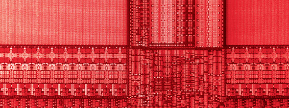
Introducing our newest innovative products for the electronics industry
Due to China’s unprecedented pace of innovation and manufacturing, we are announcing several new products at SEMICON China 2018:
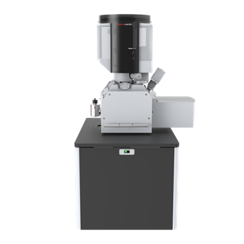
The Thermo Scientific™ Verios G4 XHR SEM (extreme high-resolution scanning electron microscope) provides manufacturers the capability and flexibility they need to determine the root causes of defects, yield losses, and process and product failures. It offers the best performance across the widest range of conditions, especially at the low voltages required for beam-sensitive materials used in advanced processes.
Learn more about Verios G4 XHR SEM ›
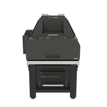
The next-generation Thermo Scientific Hyperion II System is the only nanoprober based on an atomic force microscope (AFM). This tool eliminates the vacuum requirements and e-beam/sample interactions of SEM-based nanoprobers.
Learn more about Hyperion II System ›
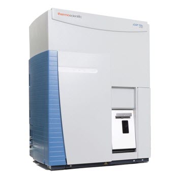
The Thermo Scientific iCAP TQs ICP-MS provides low detection limits for all relevant chemicals and yields faster measurements with less operator attention. This new system makes it possible to move chemical analysis from the lab to the fab. It also allows at-line control of chemical baths, which improves response times and minimizes contamination-related losses.
Learn more about iCAP TQs ICP-MS ›
No other company can match our breadth of knowledge and depth of technology
Thermo Fisher Scientific has proven technology for the industry roadmap from advanced finfet logic to 3D NAND to display. We are the only provider with complete analysis solutions available for every phase of the product lifecycle:
- Design Verification
Using physical and electrical analysis techniques to aid in design verification and or electrical circuit analysis testing and/or modification. Relevant techniques include Circuit Edit, Optical Fault Isolation and Compliance Testing solutions (ESD).
- Electrical Analysis
Electrical fault isolation and/or electrical failure analysis. Relevant techniques include thermal fault isolation, optical fault isolation and nanoprobing for fault isolation and/or transistor characterization.
- Physical and Elemental Analysis
Physical analysis of semiconductor structures to understand physical, elemental or structural information. Relevant techniques include SEM, TEM, EDS, XPS and Raman/FTIR analysis.
- Yield Enhancement and Process Control
Production support for high-volume wafer fabrication. Relevant techniques include SEM, TEM, EDS for yield enhancement/process control and ICPMS for inline chemical quality control.
- Incoming Quality Control
This equipment analyzes incoming materials to prevent contamination of clean room air, ultra pure water, process gases and chemicals to minimize Wafer Yield Loss. Relevant techniques include Ion Chromatography, Gas Chromatography and Trace Element Analysis.